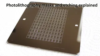
Photomasks Explained (Contact and Projection): how to etch Thin Chromium Layers
In this video, the difference between contact/proximity masks and projection masks for photolithography is discussed. These masks are used to produce MEMs and integrated circuits. In the second half of the video, I will show how to quickly etch the chromium layer off a quartz substrate.
From playlist Carl Zeiss S-planar Photolithography Lens

Photoelectric Effect, Work Function, Threshold Frequency, Wavelength, Speed & Kinetic Energy, Electr
This chemistry video tutorial explains how the photoelectric effect works. It also explains how to use the work function of metals to calculate the threshold frequency and maximum wavelength of light necessary to eject an electron off the surface of an active metal. In addition, it expla
From playlist New AP & General Chemistry Video Playlist

Engineering 165/265: Advanced Manufacturing Choices. Lec 9. STM and Atomic Force Microscopy
UCI Engineering 165/265 Mechanical and Aerospace Engineering (Spring 2014) Lec 09. Mechanical and Aerospace Engineering: Advanced Manufacturing Choices -- STM and Atomic Force Microscopy -- View the complete course: http://ocw.uci.edu/courses/mechanical_and_aerospace_engineering_165_advanc
From playlist Engineering 165/265:Advanced Manufacturing Choices

Mod-02 Lec-14 Lithography - II
Nano structured materials-synthesis, properties, self assembly and applications by Prof. A.K. Ganguli,Department of Nanotechnology,IIT Delhi.For more details on NPTEL visit http://nptel.ac.in

What is the Photoelectric Effect?
The 3rd in the series on the photoelectric effect (See my videos on Hertz and Planck - Hertz - https://www.youtube.com/watch?v=UN37QEmW_ns - Planck - https://www.youtube.com/watch?v=7hxYGaegxAM Covers how observations of the photoelectric effect lead to Einstein's theory in understanding
From playlist Nature of Light
A sample photoelectric effect / work function question with a solution
This video shows you how to use Einsteins equation for the photoelectric effect See www.physicshigh.com for all my videos and other resources. If you like this video, please press the LIKE and SHARE with your peers. And please add a COMMENT to let me know I have helped you. Follow me fac
From playlist Nature of Light

Engineering 165/265: Advanced Manufacturing Choices. Lecture 14: Laser Beam Machining + Review
UCI Engineering 165/265 Mechanical and Aerospace Engineering (Spring 2014) Lec 14. Mechanical and Aerospace Engineering: Advanced Manufacturing Choices -- Laser Beam Machining + Review -- View the complete course: http://ocw.uci.edu/courses/mechanical_and_aerospace_engineering_165_advanced
From playlist Engineering MAE 165/265: Advanced Manufacturing Choices
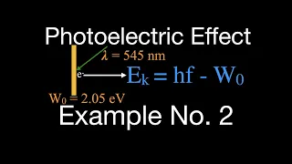
Photoelectric Effect (3 of 8 ) Example No.2 (Very Helpful)
Includes one very helpful worked example for the photoelectric effect for how to calculate the kinetic energy and velocity of the photoelectrons. The photoelectric effect is the emission of electrons when light is shined on a material. Electrons emitted in this way can be called photoelec
From playlist Quantum Mechanics
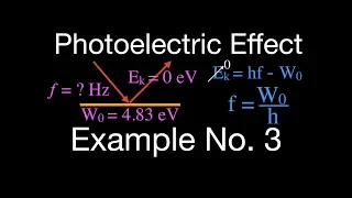
Photoelectric Effect (4 of 8) Example No.3
Includes one easy to follow worked example for the photoelectric effect showing how to determine the minimum frequency and wavelength of light needed to emit an electron from a metal with a know work function. You can see a listing of all my videos at my website, http://www.stepbystepscien
From playlist Quantum Mechanics

The physics of a laser - how it works. How the atom interacts with light. I’ll use this knowledge to simulate a working laser. We will learn how LASERs relies on Stimulated absorption, Spontaneous emission, and most importantly: Stimulated Emission- This last type interacts with an excite
From playlist New to the channel? Try these
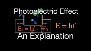
Photoelectric Effect (1 of 8) An Explanation (Clear and Simple)
Explains how the photoelectric effect works. Also includes one worked example for how to calculate the kinetic energy and velocity of the photoelectrons. The photoelectric effect is the emission of electrons when light is shined on a material. Electrons emitted in this way can be called p
From playlist Quantum Mechanics

Watch more videos on http://www.brightstorm.com/science/chemistry SUBSCRIBE FOR All OUR VIDEOS! https://www.youtube.com/subscription_center?add_user=brightstorm2 VISIT BRIGHTSTORM.com FOR TONS OF VIDEO TUTORIALS AND OTHER FEATURES! http://www.brightstorm.com/ LET'S CONNECT! Facebook ► h
From playlist Chemistry
Mod-04 Lec-40 Concluding Lecture
Nano structured materials-synthesis, properties, self assembly and applications by Prof. A.K. Ganguli,Department of Nanotechnology,IIT Delhi.For more details on NPTEL visit http://nptel.ac.in

Engineering 165/265: Advanced Manufacturing Choices. Lec 4. Thermal Machining I (Spring 2014)
UCI Engineering 165/265 Mechanical and Aerospace Engineering (Spring 2014) Lec 04. Mechanical and Aerospace Engineering: Advanced Manufacturing Choices -- Thermal Machining -- Part 1 View the complete course: http://ocw.uci.edu/courses/mechanical_and_aerospace_engineering_165_advanced_manu
From playlist Engineering 165/265:Advanced Manufacturing Choices

Quantum Transport, Lecture 4: Technology
Instructor: Sergey Frolov, University of Pittsburgh, Spring 2013 http://sergeyfrolov.wordpress.com/ Summary: This lecture reviews the three technological areas that enable the field of quantum transport. 1) crystal growth 2) nanofabrication and 3) low temperature measurements. Quantum Tran
From playlist Quantum Transport

Sarah Haigh - Probing atomic behaviour in liquids with STEM : opportunities for machine learning
Recorded 30 November 2022. Sarah Haigh of the University of Manchester presents "Probing atomic behaviour in liquids with STEM : opportunities for machine learning" at IPAM's Multi-Modal Imaging with Deep Learning and Modeling Workshop. Learn more online at: http://www.ipam.ucla.edu/progra
From playlist 2022 Multi-Modal Imaging with Deep Learning and Modeling

Mod-01 Lec-02 Introduction to Nanotechnology Contd..
Nano structured materials-synthesis, properties, self assembly and applications by Prof. A.K. Ganguli,Department of Nanotechnology,IIT Delhi.For more details on NPTEL visit http://nptel.ac.in
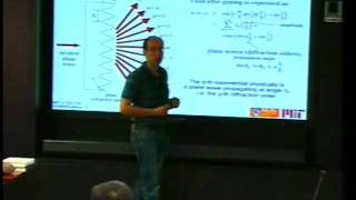
Lec 16 | MIT 2.71 Optics, Spring 2009
Lecture 16: Gratings: amplitude and phase, sinusoidal and binary Instructor: George Barbastathis, Colin Sheppard, Se Baek Oh View the complete course: http://ocw.mit.edu/2-71S09 License: Creative Commons BY-NC-SA More information at http://ocw.mit.edu/terms More courses at http:
From playlist MIT 2.71 Optics, Spring 2009

Photoelectric Effect (7 of 8) Determining Planck's Constant
An explanation of how the graph of the frequency of the incident light and the maximum kinetic energy of the photoelectrons can be used to determine Planck's constant. Also shows how to determine the work function and cutoff frequency of the photocell. You can see a listing of all my video
From playlist Quantum Mechanics

Accuracy Requirements in the Mechanical Assessment of Photonic Crystals | MIT 2.71 Optics
Accuracy Requirements in the Mechanical Assessment of Photonic Crystals Instructor: Martin Deterre, Corey Fucetola, Sebastien Uzel View the complete course: http://ocw.mit.edu/2-71S09 License: Creative Commons BY-NC-SA More information at http://ocw.mit.edu/terms More courses at
From playlist MIT 2.71 Optics, Spring 2009