https://www.patreon.com/edmundsj If you want to see more of these videos, or would like to say thanks for this one, the best way you can do that is by becoming a patron - see the link above :). And a huge thank you to all my existing patrons - you make these videos possible. In this video
From playlist Optoelectronic and Photonic Devices

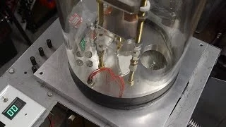
DIY Scanning Electron Microscope - Electron Gun Detail
I explain the detailed operation of the electron gun in my DIY scanning electron microscope project.
From playlist Scanning Electron Microscope

DIY Scanning Electron Microscope - Overview
Today, I finally produced an image with my DIY scanning electron microscope. I've spent the last few months working on this project, and am encouraged by today's success. There is still a lot of work left to do in making the image higher resolution, and eliminating sources of noise, howe
From playlist Scanning Electron Microscope
Electron beam control in a scanning electron microscope
I describe electron beam optics and deflection as they are employed in scanning electron microscopy. http://web.jfet.org/vclk/ - Deflection amplifier http://www.johngineer.com/blog/?p=648 - CRT Christmas tree http://www.fei.com/ - FEI Company
From playlist Scanning Electron Microscope

Physics - Optics: Polarization (1 of 5) Introduction
Visit http://ilectureonline.com for more math and science lectures! In this video I will give a short introduction to what happens to the intensity of a ray when it passes through different polarizers.
From playlist PHYSICS - OPTICS
https://www.patreon.com/edmundsj If you want to see more of these videos, or would like to say thanks for this one, the best way you can do that is by becoming a patron - see the link above :). And a huge thank you to all my existing patrons - you make these videos possible. In this video
From playlist Optoelectronic and Photonic Devices
Animation of Fermilab's Accelerator Complex
The 6,800-acre Fermilab site is home to a chain of particle accelerators that provide particle beams to numerous experiments and R&D programs. This 2-minute animation explains how the proton source provides the particles that get accelerated and travel through the accelerator complex at cl
From playlist Detectors and Accelerators

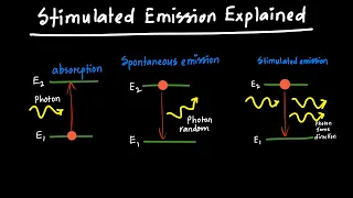
LASER Frequency Response Part 2 - Photon Rate Equation
https://www.patreon.com/edmundsj If you want to see more of these videos, or would like to say thanks for this one, the best way you can do that is by becoming a patron - see the link above :). And a huge thank you to all my existing patrons - you make these videos possible. In this video
From playlist Optoelectronic and Photonic Devices
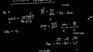
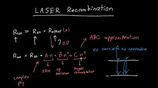
LASER Frequency Response Part 3 - Carrier Dynamics
https://www.patreon.com/edmundsj If you want to see more of these videos, or would like to say thanks for this one, the best way you can do that is by becoming a patron - see the link above :). And a huge thank you to all my existing patrons - you make these videos possible. In this video
From playlist Optoelectronic and Photonic Devices

Maxwell’s Demon Goes Optical! by Swapan Chattopadhyay
DISTINGUISHED LECTURES MAXWELL’S DEMON GOES OPTICAL! SPEAKER: Swapan Chattopadhyay (FNAL, USA & IISc, India) DATE: 15 November 2022, 17:30 to 18:30 VENUE: Chandrasekhar Auditorium Abstract: Stochastic phase space cooling using microwave techniques in the GHz frequency range have been
From playlist DISTINGUISHED LECTURES

UXSS 2016 - Dr. Agostino Marinelli
Dr. Agostino Marinelli from SLAC National Accelerator Laboratory presents "Introduction to the Physics of Free Electron Lasers" on June 13, 2016 at the Ultrafast X-ray Summer Seminar, hosted by Stanford PULSE Institute at SLAC National Accelerator Laboratory.
From playlist Stanford PULSE Institute

HEDS | Relativistic plasma mirrors for high-power ultrashort pulses from UV to soft x-ray
HEDS Seminar Series- Julia Mikhailova – June 3rd, 2021 LLNL-VIDEO-835546
From playlist High Energy Density Science Seminar Series

HEDS | Laser-driven magnetic filaments as a platform for high-field science
HEDS Seminar Series – Alexy Arefiev – July 15th, 2021 LLNL-VIDEO-836253
From playlist High Energy Density Science Seminar Series

Sarah Haigh - Probing atomic behaviour in liquids with STEM : opportunities for machine learning
Recorded 30 November 2022. Sarah Haigh of the University of Manchester presents "Probing atomic behaviour in liquids with STEM : opportunities for machine learning" at IPAM's Multi-Modal Imaging with Deep Learning and Modeling Workshop. Learn more online at: http://www.ipam.ucla.edu/progra
From playlist 2022 Multi-Modal Imaging with Deep Learning and Modeling

HEDS | Non-Maxwellian Dist Functions & their Impacts on Crossed-Beam Energy Transfer & Absorption
HEDS Seminar Series- David Turnbull – April 15th, 2021 LLNL-VIDEO-824861
From playlist High Energy Density Science Seminar Series

Quantum Transport, Lecture 4: Technology
Instructor: Sergey Frolov, University of Pittsburgh, Spring 2013 http://sergeyfrolov.wordpress.com/ Summary: This lecture reviews the three technological areas that enable the field of quantum transport. 1) crystal growth 2) nanofabrication and 3) low temperature measurements. Quantum Tran
From playlist Quantum Transport

Plasma Accelerator by Bob Bingham
06 March 2017 to 17 March 2017 VENUE: Ramanujan Lecture Hall, ICTS Bangalore Particle accelerators have been instrumental in unraveling some of the deep questions related to matter at the fundamental level, the latest being discovery of the Higgs Boson. The conventional accelerators, how
From playlist Laser Plasma Accelerator

Petar Petrov - Laser phase-contrast transmission electron microscopy & computational opportunities
Recorded 15 November 2022. Petar Petrov of the University of California, Berkeley, presents "Laser phase-contrast transmission electron microscopy and associated computational opportunities" at IPAM's Cryo-Electron Microscopy and Beyond Workshop. Abstract: A phase plate can provide optimum
From playlist 2022 Cryo-Electron Microscopy and Beyond

This video is used for Hologram technology, just make the hologram device at home with a very simple way, I'll put a video of how to make the Hologram device. Enjoy!
From playlist OPTICS
